Keyence is a direct sales company; sales people visit customers on site with demonstration cases to show products. Keyence sensors, vision systems, and high definition microscopes are part of the manufacturing and research processes in a variety of industries, including the electronics, semiconductor, automotive, food and packaging, biotechnology, and pharmaceutical industries . Keyence's customers include companies ranging from the largest Fortune 500 manufacturers to niche suppliers.
Keyence was named one
of Business Week's “1000 Best Valued Companies.” Keyence Japan is consistently
listed in the Nihon Keizai Shimbun's yearly ranking of the "Top Ten Most
Excellent Companies in Japan." Keyence is known as one of the best
"pay" companies in Japan. The average annual wage for all full-time
employees (average age: 31.9 years old) in FY2006 was JPY13,860,000 (US$117,348
as of March 2007). A 350-million-year-old ammonite fossil is displayed at the
entrance of the Japanese headquarters; other fossils of long-dead creatures
align the corridors and meeting rooms. Relics are supposed to convey a tacit
message to employees: keep aiming high or you'll become a fossil.

Keyence manufactures a
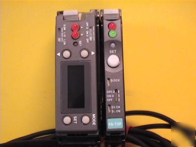
broad range of products, from photoelectric and proximity sensors to measuring
instruments for inspection lines to high precision microscopy devices used in research
institutes. These products are used by more than 80,000 customers globally.
Products are shipped from Keyence's stocking network centers in Japan, U.S.
(Chicago), the UK, Canada, Germany, Italy, France, Thailand, Malaysia,
Singapore and South Korea or from 148 agents in 31 countries on the same day of
receipt of an order. Keyence's customers in a variety of industries and
manufacturing environments use their sensor products to detect the presence or
absence of an entire part or just a particular feature of that part.
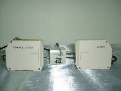
Measurement products are used to determine the size or magnitude of a
particular part or feature with great accuracy. New product releases
consistently account for 30% of Keyence's annual sales.
Vision system products are camera systems used on production
lines to differentiate and measure multiple product features. Keyence's
customers use their camera systems to perform quality control inspections that
are too complicated for ordinary sensors. The IV "Vision Sensor" is a
less expensive alternative to a full Vision system if all the capabilities of a
Vision System are not needed. Their laser marking instruments use a high
intensity laser to permanently and accurately mark shapes or characters onto
surfaces such as metals or plastics at high speeds.
- Machine Vision Sensor (IV Series)
- Machine Vision (XG Series)
- Machine Vision (CV Series)
- Laser Marker (ML Series)
- Laser Marker (MD Series)

Microscopes
are the only products offered by Keyence America for use away from a production
line. While many of the customers for their microscopes are manufacturers,
these microscopes are more typically used for research and development or
failure analysis applications. Keyence
Digital Microscopes are capable
of displaying a 3D image of the target. The image can also be manipulated or
used to make a measurement of the target feature being viewed. Their color
laser scanning microscope offers high accuracy with the use of a violet laser.
This laser microscope approaches the accuracy and resolution of an SEM at a
lower cost and without destroying the target. The information source is wikipedia .
No comments:
Post a Comment